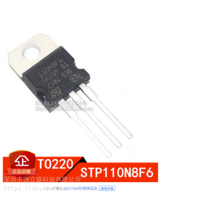
| ��Ʒ���ԣ�LOW rdson | Ʒ�ƣ�ST | �ͺţ�STP110N8F6 |
| ���ͣ���ѹIC | ��;���綯��� | ��װ��TO220 |
| ���ţ�2018+ | ��ɫ������֧�� | ��Ʒ˵����MOS |
| �Ƿ�羳��Դ���� | Ӧ�������������� |
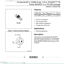
Features • Very low on-resistance • Very low gate charge • High avalanche ruggedness • Low gate drive power loss Applications • Switching applications Description This device is an N-channel Power MOSFET developed using the STripFET™ F6 technology with a new trench gate structure. The resulting Power MOSFET exhibits very low RDS(on) in all packages.
Electrical characteristics (TC = 25 °C unless otherwise specified) Table 4. On/off-state Symbol Parameter Test conditions Min. Typ. Max. Unit V(BR)DSS Drain-source breakdown voltage VGS = 0, ID = 1 mA 80 V IDSS Zero-gate voltage drain current VGS = 0, VDS = 80 V 1 µA VGS = 0, VDS = 80 V, TC = 125 °C 100 µA IGSS Gate-body leakage current VDS = 0, VGS = +20 V 100 nA VGS(th) Gate threshold voltage VDS = VGS, ID = 250 µA 2.5 4.5 V RDS(on) Static drain-source on- resistance VGS = 10 V, ID = 55 A 0.0056 0.0065 Ω Table 5. Dynamic Symbol Parameter Test conditions Min. Typ. Max. Unit Ciss Input capacitance VDS = 40 V, f = 1 MHz, VGS = 0 - 9130 - pF Coss Output capacitance - 320 - pF Crss Reverse transfer capacitance - 225 - pF Qg Total gate charge VDD = 40 V, ID = 110 A, VGS = 10 V (see Figure 14) - 150 - nC Qgs Gate-source charge - 40 - nC Qgd Gate-drain charge - 30 - nC Table 6. Switching times Symbol Parameter Test conditions Min. Typ. Max. Unit td(on) Turn-on delay time VDD = 40 V, ID = 55 A, RG = 4.7 Ω, VGS = 10 V (see Figure 13) - 24 - ns tr Rise time - 61 - ns td(off) Turn-off delay time - 162 - ns tf Fall time - 48 - ns