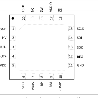
BOS1901 Piezo Haptic Driver with Digital Front End 1 Features ? High-Voltage Low Power Piezo Driver o Drives 100 nF at 190 Vpk-pk and 300 Hz with only 350 mW o Drives Capacitive Load up to 820 nF o Energy Recovery o Differential Output o Small Solution Footprint, QFN & WLCSP o Low BOM cost ? Integrated Digital Front End with SPI o 64 samples Internal FIFO Interface o 1.8 V to 5.0 V Digital I/O Supply ? Piezo Sensing ? Fast Start Up Time, <300 ?s ? Unidirectional Power Input option ? Wide Supply Voltage Range, 3 to 5.5 V 2 Applications ? Mobile Phones and Tablets ? Portable Computers ? Keyboards and Mice ? Gaming Controllers ? Wearables ? Electronic Cooling Rsense CVDD CHV L1 3.0 V to 5.5 V RM RP VDD VBUS SCLK SW HV OUT+ SPI CVDDIO CREG CS SDI SDO VDDIO REG BOS1901 GND OUT PUMP Figure 1: Simplified schematic BT001DDS01.02 – Issue 9 load CPUMP 3 Description The BOS1901 is a single-chip piezo actuator driver with energy recovery, based on a patented CapDrive? technology. It can drive actuators with up to 190 Vpk-pk waveforms while operating from a 3 to 5.5 V supply voltage. The input digital stream is written in the internal FIFO over the digital interface to generate the desired output waveform. Low power and small size make it ideal for a variety of applications requiring minimal power consumption and heat dissipation. The BOS1901 uses a high-speed SPI in its digital front end. It enables the device to share a common communication bus for multi-actuator systems and allows the user to query various data such as the actuator voltage for sensing applications (e.g. piezo buttons). The differential driver achieves low distortion waveforms and quiet actuator operation. All settings are adjustable through the digital front end to reduce the BOM. Only 7 passive discrete components are required. The BOS1901 can be operated with a wide selection of COTS inductors. In systems that cannot handle reverse current flow in the power delivery network, the BOS1901 features a Unidirectional Power Input (UPI). When the UPI mode is activated, the driver behaves as a resistive load without reducing power efficiency. Typical start-up time of less than 300 ?s makes the BOS1901 latency negligible in most systems. Safety systems protect the device from damage in case of a fault. Table 1: Ordering information PRODUCT DESCRIPTION BOS1901CQ BOS1901CW QFN 20L 4x4x0.8 mm 0.5P WLCSP 25L 2.1x2.2x0.6 mm 0.4P
Boreas Technologies 的 BOS1901 是一款专为 压电陶瓷执行器(Piezo Actuator) 设计的高效驱动芯片,其技术特点聚焦于 低功耗、高精度、微型化,适用于对能耗和尺寸敏感的应用场景。以下是其关键特性解析:
1. 核心特点
(1)***功耗设计
(2)高压输出能力
(3)高集成度
(4)精密控制
2. 典型应用场景
消费电子
智能手机摄像头对焦(OIS/AF)
TWS耳机触觉反馈(替代传统线性马达)
AR/VR设备的微动控制
医疗设备
工业自动化
3. 对比传统压电驱动方案
| 特性 | Boreas BOS1901 | 传统分立方案 |
|---|
| 功耗 | ?A级待机,50%+ 能效提升 | mA级,能量浪费严重 |
| 集成度 | 内置升压+驱动,外围简洁 | 需外置DC-DC+MOSFET |
| 控制精度 | 数字可调,支持纳米级位移 | 依赖模拟电路,精度有限 |
| 尺寸 | QFN-24(4mm×4mm) | 多芯片方案占用较大PCB面积 |
4. 设计注意事项
压电陶瓷匹配
需根据执行器容抗特性(如10nF~100nF)调整驱动频率和电压。
高压PCB布局
120V输出走线需***足够爬电距离,避免击穿或漏电。
散热管理
高频驱动时注意芯片温升,必要时增加散热铜箔。
5. 竞品与替代方案
TI DRV8662
专为触觉反馈设计,但输出电压范围较低(±200V,需双电源)。
ST LVM901
高压压电驱动,但功耗较高,无电荷回收技术。
PI(Physik Instrumente)专用驱动器
工业级高精度方案,成本较高。
6. 总结
Boreas BOS1901 的核心优势:
? 低功耗(电荷回收技术)
? 高集成度(内置120V升压,减少BOM)
? 数字可编程(I?C/SPI灵活配置)
? 微型封装(4mm×4mm QFN)
适用领域:
对功耗敏感的可穿戴设备
需静音、高精度控制的微型执行器
空间受限的嵌入式系统